
Flexible PCB Fabrication
Choose Mondo as Your Trusted Partner for Flexible PCB Fabrication, we will show our manufacturing process to you.
Flexible PCB Bulk Production
Mondo has accumulated 17 years of extensive experience in the field of Flexible PCB manufacturing. Our production team is dedicated to providing you with reliable solutions for Flexible PCB manufacturing. By partnering with us through OEM contract orders, we can become a steadfast force in expanding your business.
Flexible PCB Fabrication Process
How are flex PCBs made? Let Mondo walk you through the production process of Flexible PCB step by step. The FPC sample production process is the same as FPC mass production process.
FPC board cutting
Cut the original large area of material to the required working size.Generally, soft board materials are mostly made in roll form. In order to meet the different size requirements of products,The optimal utilization rate must be planned and designed according to different product sizes.And according to the planning results, the material is divided into the required size.

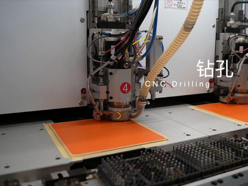
Mechanical drilling CNC Drilling
Drilling holes with required diameters are drilled on the surface of the workpiece according to customer requirements.It is convenient for plug-in, circuit conduction, welding or drilling protective film openings and positioning holes.Machinery and equipment: drilling machineMachine limitation: micro hole min Ø 0.20 mmDrilling type: round hole, milling slot hole, round hole reamingDrilling accuracy: +/-0.05 mm
Plating Through Hole
After the double/multi-layer board material is mechanically drilled, the upper and lower conductors are not really connected, and a conductive layer must be plated on the wall of the drilled hole to make the signal conductive. This process is applied to sheet structures above double-sided (double-sided conductors).
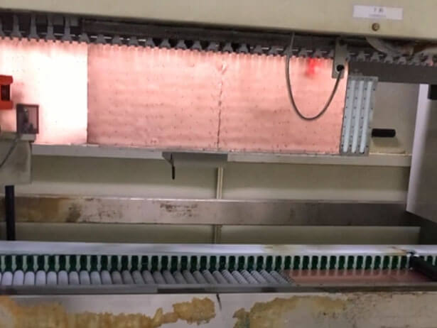
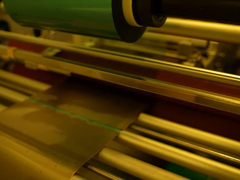
Dry Film Lamination
After the plated through hole is completed, a dry film is attached to the cleaned material by means of heating roller pressure as an etching resist.
Exposure
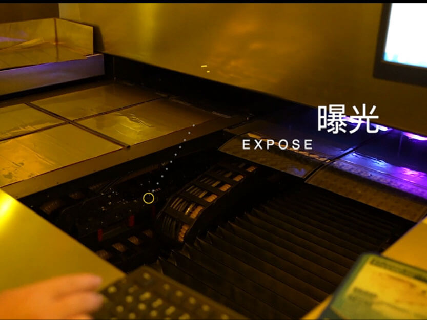
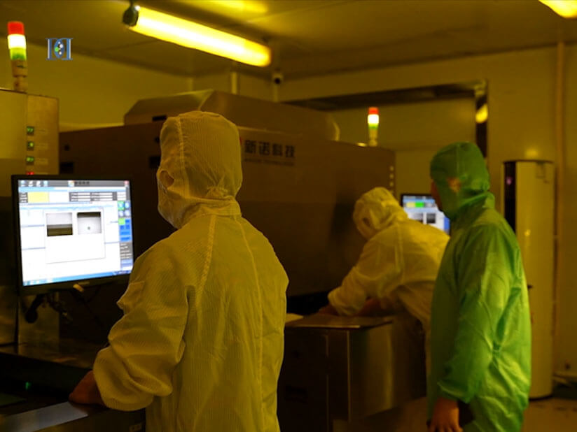
The film-finished material uses the method of image transfer to transfer the circuit pattern on the finished working film to UV exposure and transfer it to the dry film. The negative film is used for the exposure working film, and the hollowed-out light-transmitting part is the circuit and the copper-retaining area.
Developing
For the exposed material, the part of the dry film in the area irradiated by ultraviolet rays is polymerized and hardened, and after being rinsed with a specific liquid for developing, the unexposed hardened part can be washed away to expose the copper layer of the material. After developing the finished material, it can be seen that the shape and pattern of the circuit will be formed.
Etching
After the developed material is rinsed with an etching solution, the exposed part of the copper layer that is not protected by the dry film will be removed, leaving the protected circuit.
Cu+CuCl2→Cu2Cl2
Cu2Cl2+HCl+H2O2→2CuCl2+H2O

Stripping
The etched material still has a hardened dry film on the board, which is beneficial toUsing the film stripping process, the dry film is completely separated from the material, so that the circuit is completely exposed, and the copper layer is completely exposed.Stripping solution: NaOH strong alkaline solution.
Lay Up Cover Coat
A protective film (a layer of insulating material) that meets the customer’s needs is pasted on the surface of the circuit board to prevent the circuit from being oxidized and scratched, and plays a protective role.

Hot Press Lamination
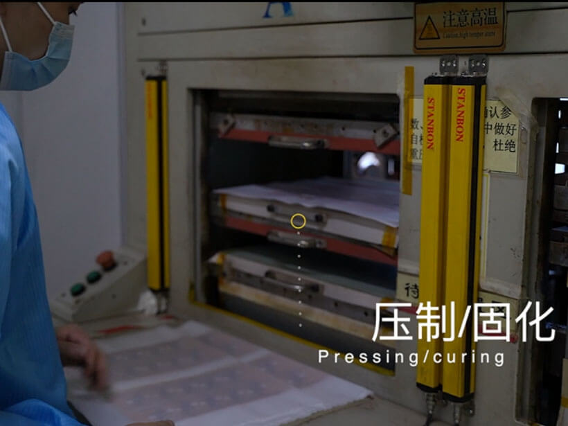
After the lamination is completed, high temperature and high pressure are provided by thermocompression, and the adhesive of the protective film is melted to fill the gap between the lines and tightly bond the copper foil material and the protective film.Working method: traditional pressing, quick pressing
Piercing
Punch out the positioning holes required by the FPC during processing.
Surface Finish
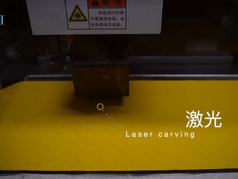
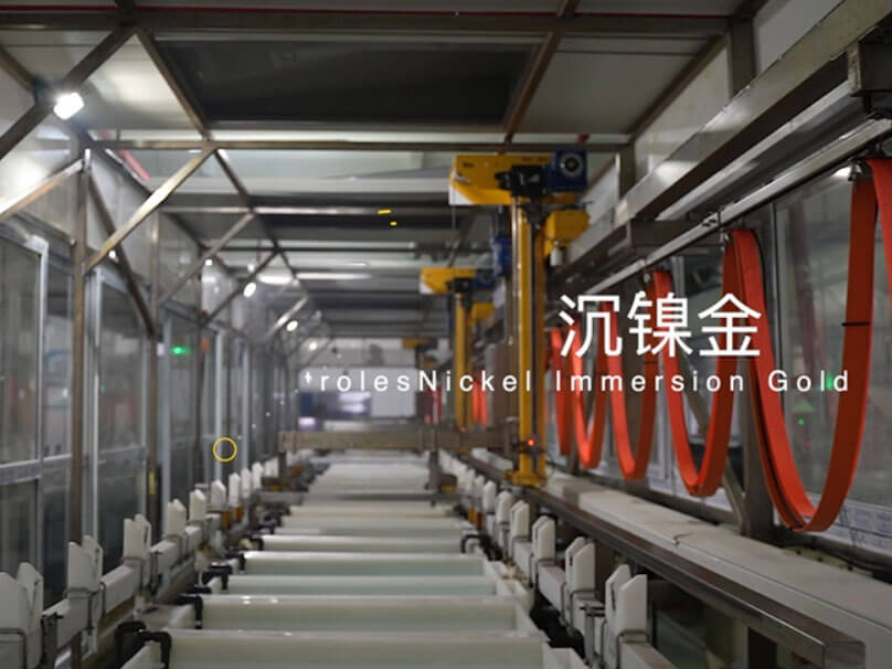
For materials completed by thermocompression, the exposed position of copper foil must be specified by the customer.Seek to be plated with different metals such as tin-lead or nickel-gold by electroplating or chemical plating to Protects exposed parts from oxidation and ensures compliance with performance requirements.
Stiffener
In order to weld parts or add reinforcement in the local area of the soft board for installationIn addition, the hard material is pressed together. Reinforcing materials are generally made of Pressure Sensitive Adhesive and The soft board is laminated but the PI reinforcement film is all hot-melt adhesive (Thermosetting) Lamination.
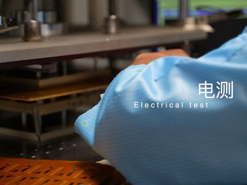
Testing
Use the probe to test whether there is an open/short circuit defect, and use the function test Check the quality of parts placement to ensure the reliability of the client.
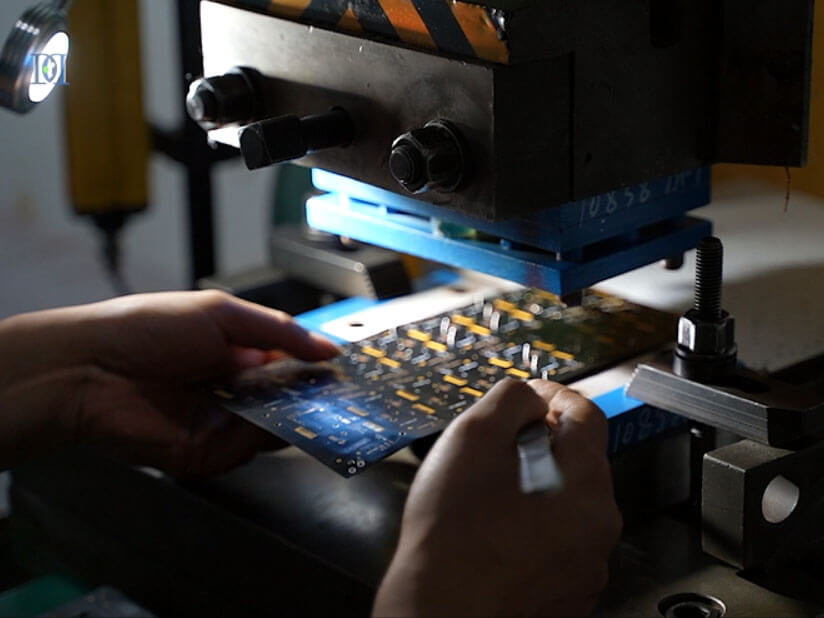
Punching
Use steel mold/knife mold or laser cutting to shape the customer’s design, No need for scrap and circuit board separation.
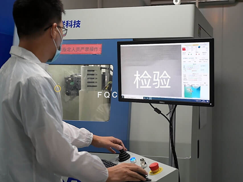
Inspection
After punching and forming, it is necessary to measure the external dimensions and check the internal defects of the circuit.But it does not affect the conduction function and the lines with poor appearance are screened out.
Process Flow
Single-sided FPC
Single-sided copper clad laminate → Cut Lamination → washing, drying → drilling or punching → screen printing line anti-etching pattern or using dry film → solidify inspection and repairing → etching copper → etching resist ink, drying → washing, drying → solder mask, UV curing → screen printing, UV curing → preheating, punching and Form → open short circuit test → washing, drying → pre-coated soldering anti-oxidant (dry) or spray hot air flattening → inspection packaging → finished product delivery.
Double-sided FPC
Double-sided copper clad laminate → Cut Lamination → lamination → CNC drilling →inspection, burr cleaning → PTH → full plate electroplated thin copper → inspection,washing → screen negative Circuit pattern, curing (dry film or wet film, exposure, developing) → inspection, repairing → line pattern plating → electroplating tin (resistance nickel/gold) → resist ink(photosensitive film) → → etching copper → (DE-WETTING) → Clean → solder mask(adhesive dry film or wet film, exposure, development, heat curing) → cleaning, drying → screen printing, curing → (HASL) → Profile → cleaning, drying → open short circuit test → inspection packaging → finished product
One-stop FPC SMT
SMT (Surface Mount Technology) is the most popular technology and process in the electronic assembly industry. With SMT assembly, components can be directly soldered onto the circuit board, making it a more efficient process.
Mondo offer a one-stop SMT assembly service. Whether you choose to purchase components on your own or through our channels, we will assist you throughout the entire assembly process until completion.
FAQ
Yes, we support low MOQ (Minimum Order Quantity) and can manufacture Flexible PCBs starting from a minimum area of one square meter.
Absolutely, we offer assistance with assembly using SMT (Surface Mount Technology) assembly techniques.
The delivery time for bulk orders may vary depending on the quantity. Generally, it takes around 7-10 working days.
We can assist you in procuring raw materials and then manufacture the products for you. Alternatively, you can send us the pre-made soft boards, and we will help you with SMT assembly.