
Flexible PCB Boards are circuit boards fabricated on flexible substrates, offering the advantages of being lightweight, thin, and flexible. This widespread application of Flexible PCB Boards requires careful and professional design, including the selection of appropriate materials, particularly in terms of size and thickness. Any mistakes in material selection can result in design flaws and render the entire product non-functional.
Base Material, Cover Material, and Adhesive
When designing a Flexible PCB Board, it is essential to consider the base material, cover material, and adhesive used in conjunction.
The base material of Flexible PCB Boards typically consists of polyimide (PI) or polyester (PET). The material thickness options range from 12.5/25/50/75/125um, with 12.5um and 25um being commonly used. If the FPC requires high-temperature soldering, PI is usually chosen as the base material, while FR4 is commonly selected as the substrate for the PCB.
The cover material of Flexible PCB Boards serves as a protective layer against contamination, moisture, and scratches. It is usually a laminated structure composed of dielectric film and adhesive or a flexible media coating. The primary materials used for the cover layer are polyimide and polyester, with a common thickness of 12.5um.
During the FPC design process, the layers need to be bonded together. This requires the use of a suitable adhesive, such as acrylic, modified epoxy resin, phenolic butyral, reinforced adhesive, or pressure-sensitive adhesive. Single-layer FPCs do not require adhesive.
In certain applications, such as device soldering, flexible boards may need external support in the form of stiffeners. Common materials used for reinforcement include PI or polyester film, glass fiber, polymer materials, steel sheets, and aluminum plates. PI or polyester film is frequently employed, with a thickness of 125um. Glass fiber (FR4) reinforced plates provide higher hardness but are more challenging to process when greater rigidity is required.
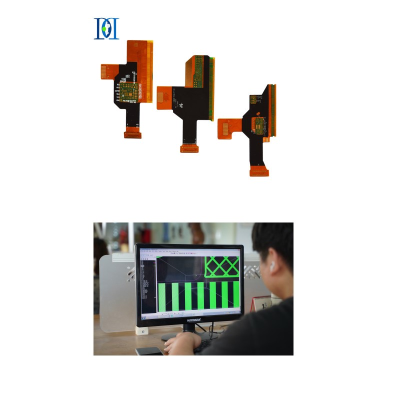
Compared with the processing methods of PCB pads, there are many processing methods of Flexible PCB Board pads
The most common are the following:
① Electroless nickel gold is also called chemical immersion gold or immersion gold. Generally, the thickness of the electroless nickel plating layer used on the copper metal surface of the PCB is 2.5um-5.0um, and the thickness of the immersion gold (99.9% pure gold) layer is 0.05um-0.1um. Technical advantages: flat surface, long storage time, easy soldering; suitable for fine pitch components and thinner PCB. For Flexible PCB Board, it is more suitable for use because of its thinner thickness. Disadvantage: Not environmentally friendly.
②The advantages of tin-lead electroplating: flat lead-tin can be added directly on the pad, which has good solderability and uniformity. For some processing technologies such as HOTBAR, this method must be used on FPC. Disadvantages: lead is easily oxidized, and the storage time is short; electroplating wires need to be pulled; not environmentally friendly.
③ Selective Gold Electroplating (SEG) refers to the use of gold electroplating in local areas of the PCB, and another surface treatment method is used in other areas. Gold electroplating means that the copper surface of the PCB is first plated with a nickel layer, and then the gold layer is plated. The thickness of the nickel layer is 2.5um-5.0um, and the thickness of the gold layer is generally 0.05um-0.1um. Advantages: The gold-plated layer is thicker, and the oxidation resistance and wear resistance are strong. “Golden fingers” generally use this processing method. Disadvantages: not environmentally friendly, cyanide pollution.
④ Organic Solderability Protective Layer (OSP) This process refers to covering the exposed PCB copper surface with a specific organic substance. Advantages: Can provide a very flat PCB surface, in line with environmental protection requirements. Suitable for PCBs with fine pitch components. Disadvantages: PCBA with conventional wave soldering and selective wave soldering process is required, and OSP surface treatment process is not allowed.
⑤Hot Air Leveling (HASL) This process refers to covering the final exposed metal surface of the PCB with 63/37 lead-tin alloy. The hot air leveling thickness of the lead-tin alloy coating is required to be 1um-25um. The hot air leveling process makes it difficult to control the thickness of the coating and the land pattern. It is not recommended to be used on PCBs with fine-pitch components, because fine-pitch components have high requirements on the flatness of the pads; the hot air leveling process is suitable for thin FPCs. The impact is high and this finish is not recommended.
In design, FPC often needs to be combined with PCB. In the connection of the two, board-to-board connectors, connectors plus gold fingers, HOTBAR, flexible and rigid boards, and manual soldering are usually used for connection. For different application environments, designers can use corresponding connection methods.
In practical applications, it is determined whether ESD shielding is required according to the application needs.
When the flexibility of FPC is not high, it can be realized with solid copper and thick dielectric. When the flexibility requirements are high, copper mesh and conductive silver paste can be used to achieve it. Due to the flexibility of FPC, it is easy to break when subjected to stress, so some special measures need to be taken to protect the FPC.
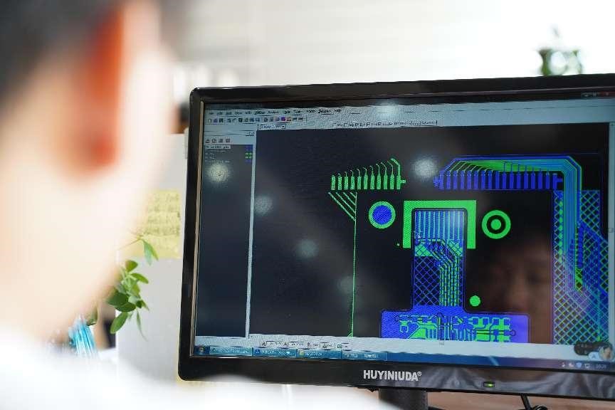
Processing Methods for Flexible PCB Board Pads
Compared to the processing methods of PCB pads, there are several common processing methods specifically used for Flexible PCB Board pads. These methods include:
- Electroless Nickel Gold (ENIG): This method involves the deposition of an electroless nickel layer followed by a thin layer of immersion gold. ENIG offers advantages such as a flat surface, good solderability, and compatibility with fine pitch components and thinner PCBs. However, it is not environmentally friendly.
- Tin-Lead Electroplating: This method provides a flat lead-tin surface with good solderability and uniformity. It is particularly suitable for processing techniques like HOTBAR. However, it has disadvantages such as lead oxidation, short storage time, and environmental concerns.
- Selective Gold Electroplating (SEG): SEG involves gold plating specific areas of the PCB while using other surface treatment methods in remaining areas. It offers a thicker gold-plated layer with excellent oxidation and wear resistance. It is commonly used for “golden fingers” but is not environmentally friendly due to cyanide pollution.
- Organic Solderability Protective Layer (OSP): OSP involves applying a specific organic substance to cover the exposed copper surface of the PCB. It provides a flat surface and complies with environmental requirements. However, it requires specific soldering processes and is not suitable for conventional wave soldering or selective wave soldering.
- Hot Air Leveling (HASL): HASL covers the exposed metal surface of the PCB with a lead-tin alloy. It is not recommended for fine-pitch components due to difficulties in controlling coating thickness and pad flatness. It is more suitable for thin FPCs but has a significant impact and is not recommended.
In FPC design, various methods are used to connect FPC with PCB, such as board-to-board connectors, connectors with gold fingers, HOTBAR, flexible and rigid boards, and manual soldering, depending on the application requirements.
ESD shielding is determined based on specific application needs.
For FPCs with lower flexibility requirements, solid copper and thick dielectric materials can be used. For higher flexibility requirements, copper mesh and conductive silver paste can be employed. Special measures should be taken to protect FPCs from stress-induced breakage due to their inherent flexibility.
Routing Considerations for Flexible PCB Boards
Due to the unique characteristics of Flexible PCB Boards, it is crucial to pay attention to the following points when routing:
- Wiring Rules: Prioritize smooth signal wiring and adhere to the principles of short, straight, and fewer vias. Avoid long, thin, and rounded traces, and focus on horizontal, vertical, and 45-degree lines. Follow the arc line with the bent part.
Detailed considerations are as follows:
- Line Width: Consider the varying line width requirements of data lines and power lines, and allocate an average of 0.15mm for wiring space.
- Line Spacing: Set the design line spacing (Pitch) to 0.10mm, considering the current production capacity of most manufacturers.
- Line Clearance: Maintain a distance of 0.30mm between the outermost line and the Flexible PCB Board outline. Provide as much space as possible.
- Fillet: Use a minimum fillet design with a radius (R) of 1.5mm for the Flexible PCB Board profile.
- Wire Orientation: Ensure that the wires are perpendicular to the bending direction.
- Even Distribution: Pass the wires evenly through the bending area.
- Coverage in Bending Area: Aim to cover the bending area with wires as much as possible.
- Avoid Additional Plated Metal: No additional plated metal should be present in the bend area (unplated wires in the bend area).
- Consistent Line Widths: Maintain consistent line widths throughout the design.
- Avoid Overlapping Traces: Prevent traces on double-sided boards from overlapping and forming an “I” shape.
- Minimize Layers in the Bending Area: Reduce the number of layers in the bend area whenever possible.
- No Vias or Metallization Holes: Avoid placing vias and metallization holes in the bending area.
- Bending Center Axis: Set the bending center axis in the center of the wire. Strive for consistency in material coefficients and thicknesses on both sides of the wire, especially for dynamic bending applications.
- Horizontal Plane Twist: Reduce the bending section or increase the flexibility by partially increasing the copper foil area.
- Vertical Bending: Increase the bending radius and minimize the number of layers in the central area of the bend for vertical bending.
- EMI Considerations: For products with EMI requirements and high-frequency radiation signal lines like USB and MIPI, consider adding a conductive silver foil layer to the Flexible PCB Board. Ground the conductive silver foil based on EMI measurement results.
Summary of points to note
FPC design requires simultaneous consideration of the substrate, cover material, and adhesive. It also involves taking into account the complex processing involved in Flexible PCB Board. Additionally, attention must be given to thickness, line spacing, and board size in Flexible PCB Board design. Due to the unique nature of Flexible PCB Board, special attention should be paid to these points during the design process.