
I'm sure you're familiar with 3D printers, but using them to DIY flexible PCBs (FPCs) may be a little unknown to you. In fact, flexible PCBs can be etched using a 3D printer, regardless of the thickness of the copper foil or even if it's just a piece of conductive cloth material. Common flexible PCB materials of any thickness, such as FR4, can also be etched using this method.
Step 1: Designing method
PLA, nylon, ABS, and most consumables are difficult to effectively stick to copper foil with a 2D printer, making it challenging to etch them into the desired flexible PCBs. However, Ninjaflex material is up to the task, adhering to almost anything, including acrylic, blue printing tape, and glass.
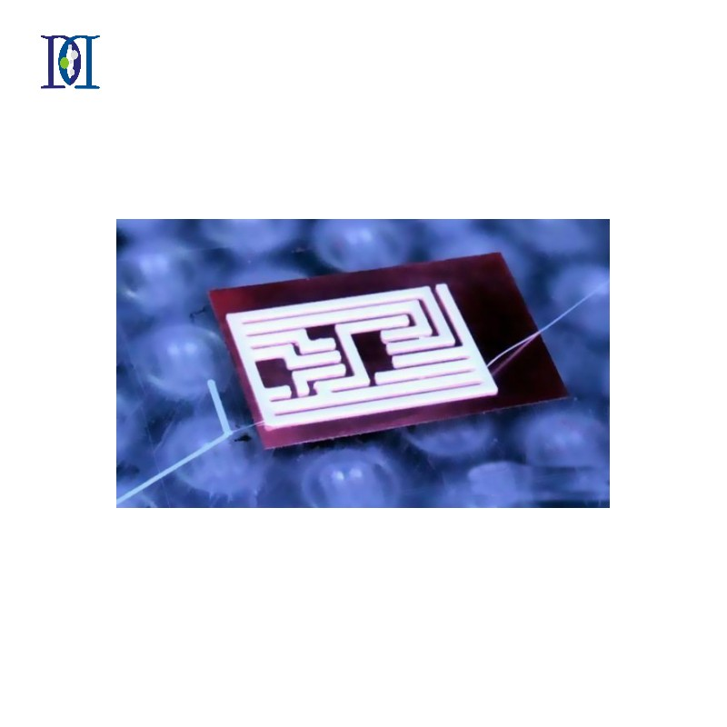
The wiring for the flexible PCBs can be drawn using free software like 123D Design, which draws the wiring on a copper foil sheet or conductive cloth. As seen in the first picture, it is not difficult to use common ferric chloride etching methods.
The above picture displays the DIY flexible PCBs and the perforated board, with holes centered 0.1 inch apart, matching other 0.1″ standard pin center distance elements. The second image shows the finished circuit board, a Picaxe microcontroller.
If you want to design a light and thin flexible PCB, that’s fine. However, these devices need to be designed much more carefully if they are highly circumferential.

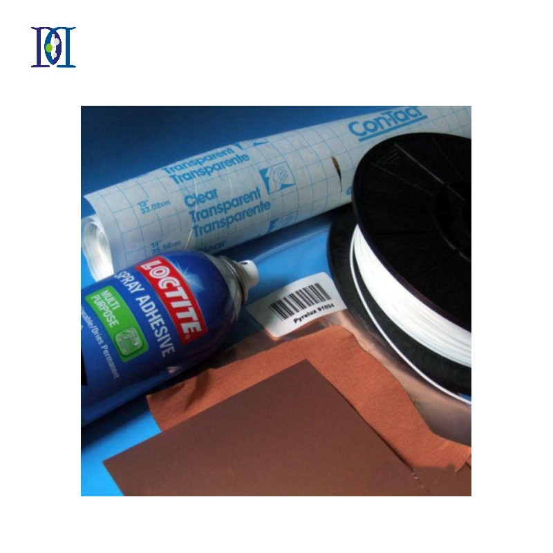
Step 2: Prepare your materials
Now, I need to prepare the 3D printing supplies. I used the Makerbot Replicator 2, but other printers with the same extruder will work as well. Ninjaflex in white is the recommended material, as black and clear Ninjaflex have been tried before but do not adhere as well. You could try another color. The basic tools and materials required are as follows:
- Scissors
- Pure copper polyester Taff fabric (0.02 inches)
- Ultra-thin copper foil circuit board (less than 0.01 inch)
- Clean lining material
- Loctite gum
- 123D Design or other 3D software that can generate and run STL files
- Ferric chloride (or other etching fluids)
- Steel wire ball
- Acetone
- Duct tape.
Step 3: Design the flexible pcbs
Plotting a line:
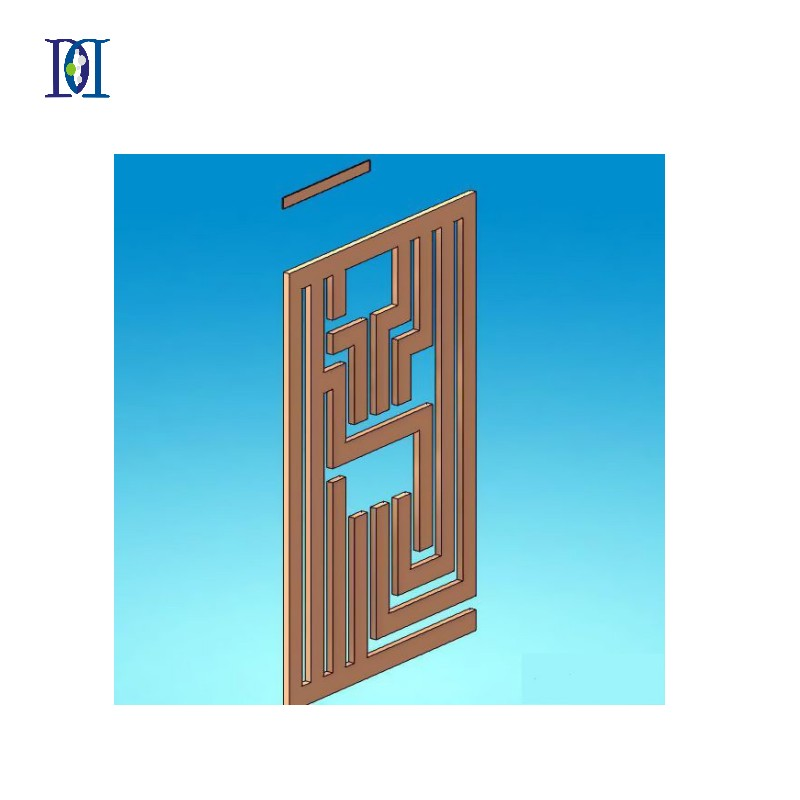
123D Design is capable of designing lines and graphics. After drawing the graphics, the film will be sprayed to a thickness of 0.011 inches. The 0.06 inch line width and 0.04 inch line spacing are standard values that match the pin spacing of the component.
Using isolation strips:
An isolation strip should be added to the side of the drawing pattern. When printing the pattern, the isolation strip can be adjusted according to the thickness of different flexible PCB materials. It can be made up to 0.7 inches. If a thicker sheet is required, the bottom strip will need to be pressed down to achieve the appropriate thickness.
Step 4: Adjust the 3D printer
Ninjaflex printers need to be adjusted if using Ninjaflex materials for printing.
Checking the extruder:
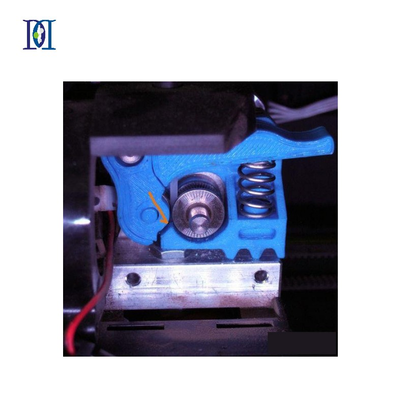
The extruder should be properly adjusted before printing with Ninjaflex. If using Makerbot’s old Replicator 2 printer, install an extended kit and download a Thingiverse driver for it. If using another printer model, make sure the Thingiverse driver is compatible with your printer. A small gap between the bearing and the gear can cause many problems.
Balancing the machine tool:
The plating error on copper foil is only allowed within a small range. If the spray does not stick well, subsequent etching will not be complete. Therefore, the machine must be kept very flat and level. The tool can be adjusted with a standard scale printed in the middle of the machine, and a margin of error of 0.02 inches must be maintained at the end of each print.
Running a print test:
Print directly on the machine tool, mark the edges of the figure, and then peel the figure. This will allow you to crop it to an FPC.
Setting up Replicator 2:
If using Replicator 2, set it up as follows:
- Infill: 100%
- Shells: 2
- Layer height: 0.2mm
- Temperature: 225°C
- Extruding speed: 15mm/s
- Traveling speed: 150mm/s
- Fill: 100%
- Height: 2mm
- Extruding speed: 15mm/s
- Traveling speed: 150mm/s
Step 5: Secure the circuit board
The flexible PCB material to be printed must be flat and level on the machine tool, and the only way to achieve this is by using spray glue. Before fixing it, wipe off the oxide layer of the board.

Step 6: Print the flexible pcbs
After printing the flexible PCBs, check whether the ink is effectively adhered to the circuit board. If the spacing is too small, you will need to adjust the STL file in 123D Design and thicken the isolation strip.
Step 7: Etch the circuit board
After removing the board from the printer, be careful not to squeeze the Ninjaflex. Then, clean the machine.
To clean the residual glue at the bottom of the flexible PCB board, use acetone. This helps ensure that the bottom of the copper foil can be etched thoroughly. The next step is to place the flexible PCBs in a standard ferric chloride etching solution.

Step 8: Etch conductive cloth
Etching conductive cloth can produce flexible PCBs with better folding, which is useful for circuits that require repeated bending. The etching process is the same as the above method, with the addition of one point: a reinforcing plate should be added to the bottom of the circuit board. If the thickness of the conductive cloth and reinforcing plate is greater than 0.007 inches, the isolation strip will need to be adjusted. The etching speed of conductive cloth takes only about 5 minutes.

Step 9: Closing remarks
The circuit center spacing of the above flexible PCB sample is 0.1 inch. The narrowest one we have made so far has a line width of 0.03 inches and a line spacing of 0.05 inches. This spacing is suitable for fabricating SOIC circuits.
Ninjaflex can print almost anything and is excellent for its adhesion and flexibility.
