
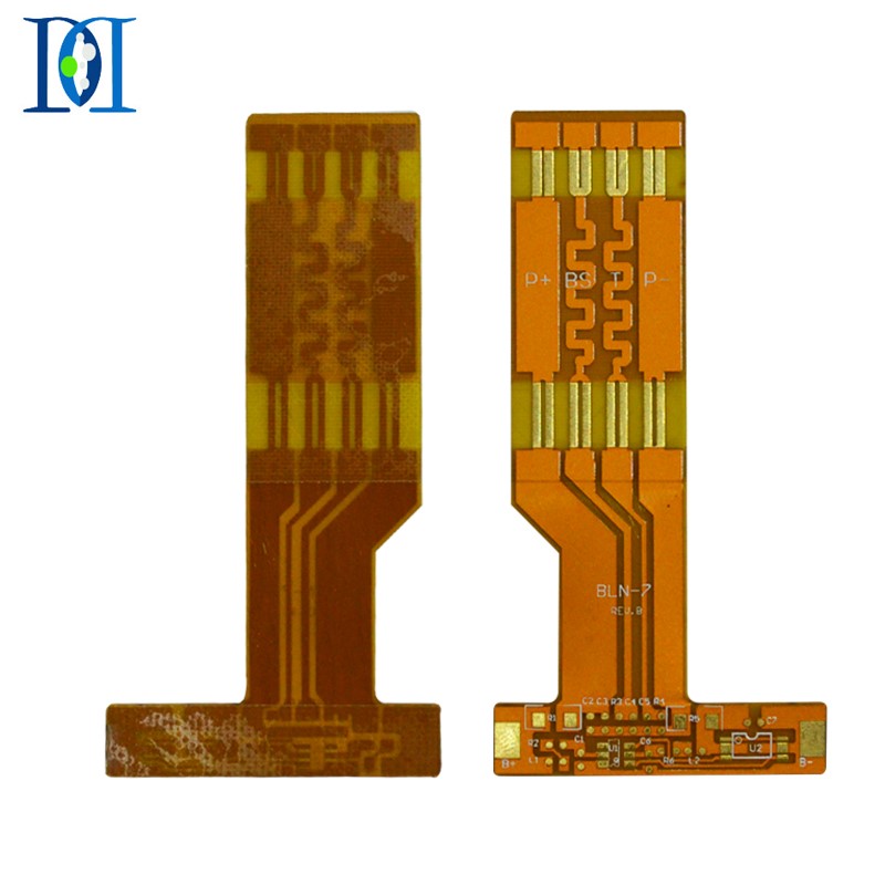
Flexible PCB boards are a technology that originated in the United States during the 1970s for the advancement of space rocket technology. This technology involves embedding circuit designs onto thin and lightweight plastic sheets, allowing for the integration of numerous precision components within a narrow and restricted space, creating a flexible flex circuit.So, what are the precautions for flexible PCB board manufacturing operations?
Constituent Material?
1. Insulating Film
The insulating film serves as the base layer of the circuit, and the adhesive is used to bond the copper foil to the insulating layer. In multi-layer designs, it is then bonded to the inner layer. These films also provide protection against dust and moisture, as well as reducing stress during flexing. The copper foil forms a conductive layer.
In certain flexible PCBs, rigid members made of aluminum or stainless steel are utilized to provide dimensional stability, physical support for component and wire placement, and stress relief. The adhesive is used to bond the rigid member and the flexible circuit together. Another material occasionally used in flexible circuits is an adhesive layer, which is created by applying adhesive to both sides of an insulating film. Adhesive layers offer environmental protection, electrical insulation, and the ability to eliminate a single film, as well as bonding multiple layers with fewer
2. Conductor
Copper foil is commonly employed in flexible circuits and can be either electrodeposited (ED) or plated. Electrodeposited copper foil has a glossy surface on one side, while the processed surface on the other side is dull. It is a flexible material that can be manufactured in various thicknesses and widths. The matte side of ED copper foil is often specially treated to enhance adhesion. Wrought copper foil, in addition to its flexibility, possesses hardness and smoothness, making it suitable for applications requiring dynamic deflection.
3. Adhesive
In addition to bonding insulating films to conductive materials, adhesives can also function as overlays, protective coatings, and overlay coatings. The key distinction lies in their application. The cover layer is used to bond the insulating film together, forming the circuit in a laminated construction. Overlay coatings of adhesive are applied using a screen printing technique.
Not all laminate structures contain adhesives, and adhesiveless laminates result in thinner circuits and increased flexibility. They also exhibit better thermal conductivity compared to adhesive-based laminate constructions. The thin structure of adhesiveless flex circuits, coupled with improved thermal conductivity due to the absence of adhesive’s thermal resistance, enables their utilization in working environments where adhesive-based flex circuits cannot be employed.
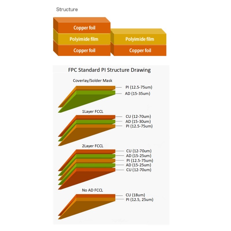
Copper Foil Substrate: Copper Film
- Copper Foil: It is divided into two main types: electrolytic copper and rolled copper. Common thicknesses include 1oz, 1/2oz, and 1/3oz.
- Substrate Film: Common thicknesses are 1mil and 1/2mil.
- Adhesive: The glue used, and its thickness is determined based on customer requirements.
- Cover Film/Protective Film: The cover film is used for surface insulation, with common thicknesses of 1mil and 1/2mil.
- Release Paper: It prevents the adhesive from sticking to foreign materials before pressing and facilitates the operation process.
- Reinforcing Board: PI Stiffener Film, which enhances the mechanical strength of the FPC and facilitates surface mounting operations. Common thicknesses range from 3 mil to 9 mil.
- EMI: Electromagnetic Shielding Film, which protects the circuit inside the circuit board from interference caused by the external environment, such as strong electromagnetic fields or susceptible areas.
How to solder?
1. Operation Steps
(1) Before soldering, apply flux to the pad and treat it with a soldering iron to prevent poor tin plating or oxidation of the pad, which can result in poor soldering. Generally, the chip does not need any special treatment.
(2) Carefully position the PQFP chip on the PCB using tweezers, taking care not to damage the pins. Align the chip with the pads, ensuring correct orientation. Adjust the temperature of the soldering iron to at least 300 degrees Celsius. Apply a small amount of solder to the tip of the iron, press down on the aligned chip with a tool, and add a small amount of flux to the pins at two opposite corners. Hold the chip in place and solder the pins on the two opposite corners to secure the chip. After soldering the diagonal corners, recheck the alignment of the chip. Make any necessary adjustments or remove and realign it on the PCB.
(3) When soldering all the pins, add solder to the tip of the soldering iron and apply flux to all the pins to keep them wet. Touch the tip of the soldering iron to the end of each pin until you see solder flowing into the pin. While soldering, keep the tip of the soldering iron parallel to the pins to prevent excess solder and overlapping.
(4) After soldering all the pins, apply flux to clean the solder on all the pins. Remove any excess solder where needed to eliminate shorts or overlaps. Finally, use tweezers to check for any solder bridges. After completing the inspection, remove the flux from the circuit board. Dip a bristle brush in alcohol and carefully wipe it along the direction of the pins until the flux disappears.
(5) Soldering SMD RC components is relatively easy. Apply solder to a solder joint first and then position one end of the component. Hold the component in place with tweezers and solder one end. Check if it is correctly positioned. If so, solder the other end.
2. Matters Needing Attention
In terms of layout, when the circuit board size is too large, it may make soldering easier to control, but it also results in long printed lines, increased impedance, decreased anti-noise ability, and higher costs. On the other hand, if the board size is too small, heat dissipation decreases, soldering becomes difficult to control, and adjacent lines are more prone to mutual interference, such as electromagnetic interference.
Therefore, PCB board design should be optimized as follows:
- Shorten the connections between high-frequency components to reduce EMI interference.
- Use brackets to secure components with heavy weight (e.g., more than 20g) before soldering.
- Consider heat dissipation for heating elements to prevent defects and rework caused by large temperature differences (ΔT) on the surface of the element. Keep thermal elements away from heat sources.
- Arrange components as parallel as possible for aesthetic appeal, ease of soldering, and suitability for mass production. The board can be designed as a 4:3 rectangle.
- Avoid abrupt changes in wire width to prevent wiring discontinuities.
- For flexible PCB boards, it is important to note that long-term heating can cause the copper foil to expand and detach. Therefore, the use of large-area copper foil should be avoided.
If you have further questions about flexible PCB production and require detailed professional guidance and advice, it is recommended to consult a professional flexible PCB manufacturer and send an inquiry to receive professional assistance.